Microvia PCB FAQ

Typical laser via diameter?

Usually 75 to 100 micrometres, set by dielectric thickness and laser process window.

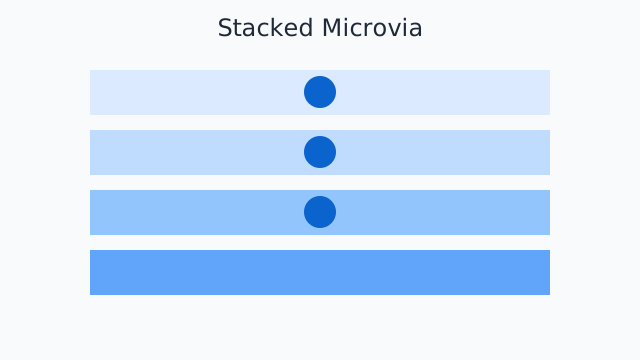
When is a stacked microvia worth it?

When routing density under a fine-pitch BGA leaves no room to stagger, and the build can carry the extra lamination and plating control.

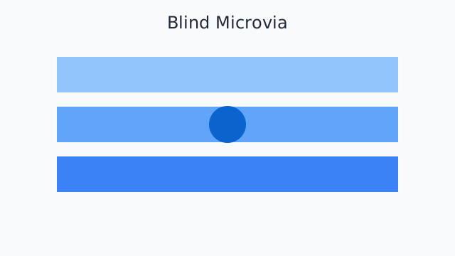
Faq - Blind microvia landing on the layer-2 capture pad
Blind microvia landing on the layer-2 capture pad
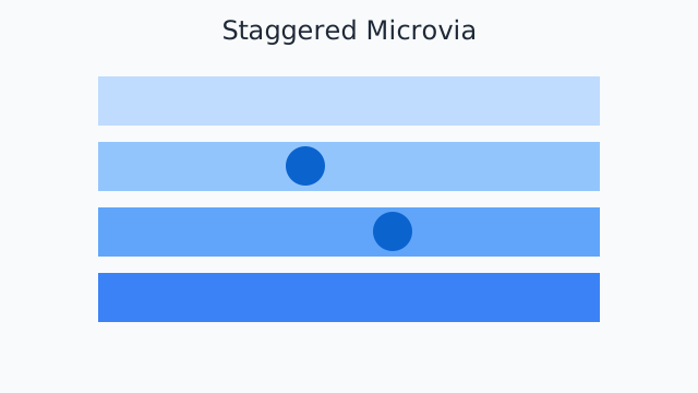
Faq - Staggered microvia transition across build-up layers
Staggered microvia transition across build-up layers
Faq - Stacked microvia column through three build-up layers
Stacked microvia column through three build-up layers

Need a Microvia PCB quotation?

Send stack-up and Gerber data to get engineering feedback and pricing.
Get Microvia PCB Quote WhatsApp: +86 136 00427328